Vertical Compute and imec aim to stack memory directly over logic to slash on-chip data movement
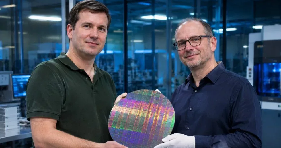
While AI hardware discussions often focus on larger models and faster accelerators, a critical bottleneck remains just millimeters away: the energy and time consumed moving data between memory and logic. To address this, European startup Vertical Compute and imec have announced an expanded partnership to advance the commercial manufacturing of Vertically Integrated Memory (VIM), a technology designed to drastically reduce data movement distances within the chip.
The core concept is straightforward, but the execution is highly complex. Vertical Compute aims to integrate high-density magnetic memory directly on top of compute logic, rather than connecting memory and compute as separate components or via long-distance interconnects. By reducing data paths from centimeters to a few dozen nanometers, the technology promises lower latency, reduced energy loss, and decreased reliance on expensive external high-bandwidth memory (HBM). However, as with most architectural shifts, there remains a significant gap between these announcements and a market-ready product.
Addressing the AI Memory Wall
As AI models grow and workloads become more data-intensive, the ratio between compute power and memory bandwidth becomes a primary constraint. A processor can only operate efficiently if data arrives quickly and results can be stored without excessive travel. In traditional systems, logic and memory are spatially separated, requiring data to move across package connections, traces, or other interconnects—a process that consumes energy, increases latency, and limits system scalability. For AI, where massive memory access is the norm, this movement often becomes the ultimate bottleneck.
Vertical Compute’s VIM approach falls into the broader category of 'Memory-near-Compute' or 'Memory-on-Logic' architectures. Unlike tightly coupled external memory, VIM focuses on vertical integration. By stacking high-density magnetic memory directly above the logic and integrating it within a unified manufacturing flow, data is stored and accessed exactly where the computation occurs. This shift from 'data movement' to 'data proximity' aims to tackle the root cause of energy and latency issues, though the technical challenge of mastering memory technology, logic processes, and integration simultaneously is immense.
From 40nm Test Chips to 16nm Pre-production
The partnership between Vertical Compute and imec moves beyond mere R&D into a more integrated engineering model. The roadmap focuses on two specific milestones: the full validation of an existing 40nm test chip and the preparation of the first pre-production product using a 16nm process. According to the companies, the 16nm logic will be manufactured at a commercial foundry, while the proprietary VIM memory layer will be added directly at imec. This transition is supported by the EU-funded NanoIC pilot line, which is designed to bridge the gap between advanced semiconductor research and industrial-scale manufacturing.
This transition is a critical hurdle for new memory architectures. Many concepts succeed in a laboratory setting but fail during the move to reproducible manufacturing due to complexity, cost, or process incompatibility. The VIM roadmap is significant because it outlines a concrete path from 40nm validation toward 16nm pre-production, rather than just presenting a theoretical concept.
The Competitive Landscape and European Strategy
To understand VIM's positioning, it must be compared to existing hierarchies. SRAM is extremely fast and sits near logic but occupies significant die area. DRAM offers much higher density but is slower and spatially distant from logic. High Bandwidth Memory (HBM) shortens these paths through stacked dies and wide interconnects, yet it remains an external component within the package environment, making it expensive and complex. VIM seeks to bypass these trade-offs by moving the memory into the logic stack itself.
While the benefits of reduced latency and lower infrastructure costs are clearly stated by the developers, it is important to note that no independent benchmarks or performance measurements have been published to verify the actual scale of these improvements. Furthermore, the ultimate application of VIM—whether as an accelerator supplement, a specialized Edge AI component, or a foundation for broader computing architectures—remains an open question.
Strategically, this project highlights the European effort to move from semiconductor research to scalable industrial production. The NanoIC pilot line, funded by the Chips Joint Undertaking and participating states including Belgium, France, Germany, Finland, Ireland, and Romania, serves as a vital test case for whether such infrastructure can successfully transition novel architectures into the commercial market.
The core concept of Vertically Integrated Memory (VIM) is straightforward, but the execution is highly complex. Vertical Compute aims to integrate high-density magnetic memory directly on top of compute logic, rather than connecting memory and compute as separate components or via long-distance interconnects. By reducing data paths from centimeters to a few dozen nanometers, the technology promises lower latency, reduced energy loss, and decreased reliance on expensive external high-bandwidth memory (HBM). However, as with most architectural shifts, there remains a significant gap between these announcements and a market-ready product.
Addressing the AI Memory Wall
As AI models grow and workloads become more data-intensive, the ratio between compute power and memory bandwidth becomes a primary constraint. A processor can only operate efficiently if data arrives quickly and results can be stored without excessive travel. In traditional systems, logic and memory are spatially separated, requiring data to move across package connections, traces, or other interconnects—a process that consumes energy, increases latency, and limits system scalability. For AI, where massive memory access is the norm, this movement often becomes the ultimate bottleneck.
Vertical Compute’s VIM approach falls into the broader category of 'Memory-near-Compute' or 'Memory-on-Logic' architectures. Unlike tightly coupled external memory, VIM focuses on vertical integration. By stacking high-density magnetic memory directly above the logic and integrating it within a unified manufacturing flow, data is stored and accessed exactly where the computation occurs. This shift from 'data movement' to 'data proximity' aims to tackle the root cause of energy and latency issues, though the technical challenge of mastering memory technology, logic processes, and integration simultaneously is immense.
From 40nm Test Chips to 16nm Pre-production
The partnership between Vertical Compute and imec moves beyond mere R&D into a more integrated engineering model. The roadmap focuses on two specific milestones: the full validation of an existing 40nm test chip and the preparation of the first pre-production product using a 16nm process. According to the companies, the 16nm logic will be manufactured at a commercial foundry, while the proprietary VIM memory layer will be added directly at imec. This transition is supported by the EU-funded NanoIC pilot line, which is designed to bridge the gap between advanced semiconductor research and industrial-scale manufacturing.
This transition is a critical hurdle for new memory architectures. Many concepts succeed in a laboratory setting but fail during the move to reproducible manufacturing due to complexity, cost, or process incompatibility. The VIM roadmap is significant because it outlines a concrete path from 40nm validation toward 16nm pre-production, rather than just presenting a theoretical concept.
The Competitive Landscape and European Strategy
To understand VIM's positioning, it must be compared to existing hierarchies. SRAM is extremely fast and sits near logic but occupies significant die area. DRAM offers much higher density but is slower and spatially distant from logic. High Bandwidth Memory (HBM) shortens these paths through stacked dies and wide interconnects, yet it remains an external component within the package environment, making it expensive and complex. VIM seeks to bypass these trade-offs by moving the memory into the logic stack itself.
While the benefits of reduced latency and lower infrastructure costs are clearly stated by the developers, it is important to note that no independent benchmarks or performance measurements have been published to verify the actual scale of these improvements. Furthermore, the ultimate application of VIM—whether as an accelerator supplement, a specialized Edge AI component, or a foundation for entirely new types of computing systems—remains to be seen. The current announcement is an ambitious development plan, including 40nm validation, 16nm pre-production, and European pilot line support, rather than proof of a market-ready memory revolution.