
Sony and TSMC Build Joint Chip Fab for $6.3 Billion to Supply Next-Gen CMOS Sensors
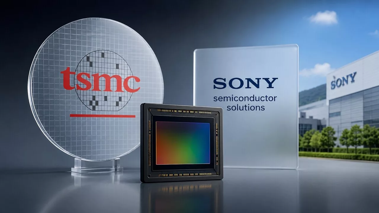
According to Nikkei Asia, the new facility will be built on the site of an existing Sony Semiconductor Solutions plant in Koshi, Kumamoto Prefecture, Japan. The total investment is estimated at around 1 trillion yen, or approximately $6.3 billion. Ownership structure sees Sony controlling roughly 60% of the joint venture, while TSMC takes about a 40% stake.
Mass production of the new sensors is scheduled to begin as early as 2029. This collaboration aims not only to upgrade smartphone camera capabilities but also to supply more powerful image sensors for future generations of Apple's iPhone. Furthermore, the partnership targets the emerging field of "Physical AI," where AI systems control physical objects like robots and vehicles rather than just executing digital tasks.
For Sony, this deal aligns with its strategy to adopt a "Fab-Light" model. As CEO Hiroki Totoki noted, the cooperation allows the company to reduce capital binding on its own production facilities by sharing costs and responsibilities.
Technologically, the partnership does not imply that Sony will share its core manufacturing secrets with TSMC. The Japanese conglomerate intends to keep certain proprietary processes that underpin its sensor leadership confidential. In return, TSMC will contribute its expertise in advanced manufacturing processes and expand its know-how in image sensors.
The choice of Kumamoto is strategic: the region offers sufficient water resources for chip production and access to relatively cheap renewable energy from geothermal and solar sources. TSMC already operates its first Japanese fabrication site there and plans further long-term investments in the area.
Гика
