

Micron to adopt 4F²-cell exit, 1δ manufacturing, and High-NA EUV

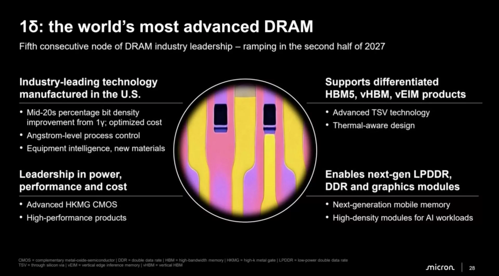
During a recent webinar, Micron detailed its future manufacturing roadmap, revealing specific technical shifts for its DRAM production. The company is currently ramping up its 1δ (1-Delta) process, which is set to succeed the 1γ (1-Gamma) generation, with mass production expected to begin in the second half of 2027 at the Boise facility in Idaho.
The Path to Angstrom-Scale Manufacturing
The 1δ (1-Delta) generation aims to increase memory density by approximately 25% compared to the 1γ (1-Gamma) process. This density boost is intended to lower the cost per bit by fitting more data into the same silicon area. To achieve this, Micron is leveraging advanced EUV lithography with angstrom-level process control, new materials, and optimized HKMG (High-k Metal Gate CMOS) technology to improve both speed and power efficiency.
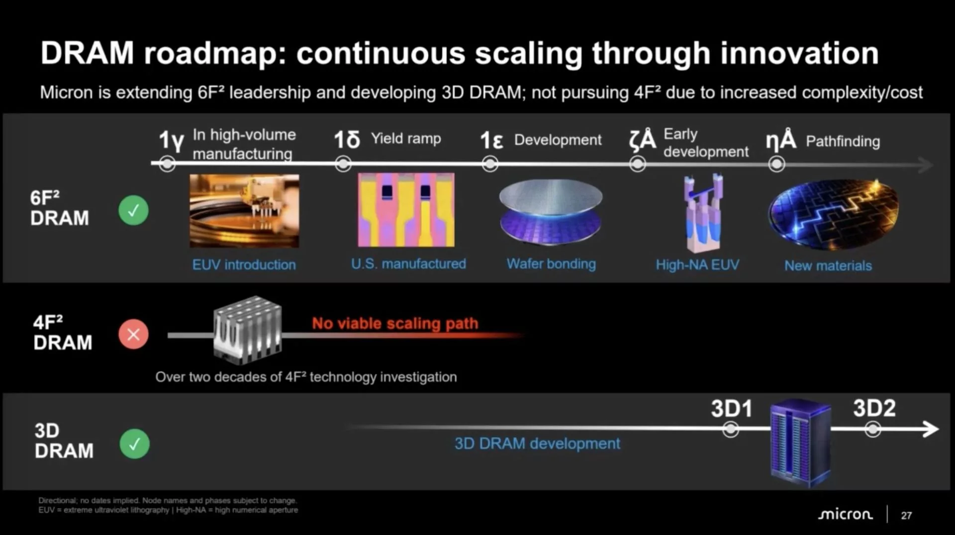
Looking further ahead, the roadmap includes the 1ε (1-Epsilon) process involving Wafer Bonding, and the early-stage 1ζ (1-Zeta) generation, which is expected to utilize High-NA EUV lithography. For the 1η (1-Eta) generation, the company is already engaging in "Pathfinding" to consider entirely new technologies.
The Shift from 4F² to 6F² Architecture
One of the most significant technical decisions is the move away from 4F² technology. Despite over 20 years of research and the production of prototypes, Micron does not see 4F² as a viable long-term development path, opting instead for the 6F² architecture. The core argument is that the capacitor pitch—the distance between capacitors—is the ultimate limiting factor for memory density, rather than the nominal footprint of the transistor alone. This approach differs from SK hynix, which presented a 4F² DRAM cell with a vertical gate in June 2026 to overcome scaling limits.
Advanced Packaging and Vertical HBM
Micron is also working on new packaging technologies to enhance bandwidth and efficiency for future HBM generations, including HBM5, vHBM, and vEIM. A key focus is increasing interconnect density through reduced Through-Silicon Via (TSV) and microbump dimensions. For stacks up to 16 layers, Micron plans to combine microbumps with Hybrid Copper Bonding to connect dies almost without gaps.
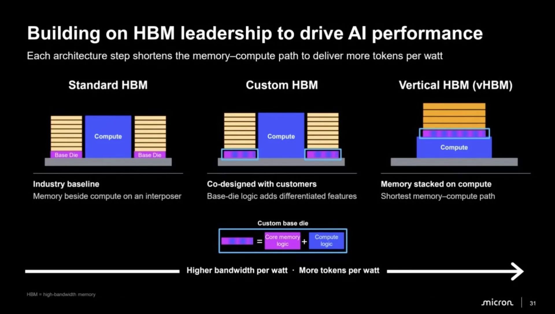
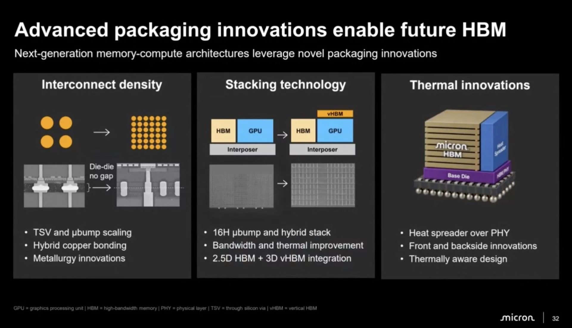
The most ambitious concept is Vertical HBM (vHBM). While traditional HBM places memory stacks next to the GPU on a shared interposer, vHBM aims to stack memory directly on top of the computing unit. This integration of 2.5D packaging with a vertical 3D arrangement is intended to shorten electrical paths, enabling higher bandwidth and lower power consumption, particularly for AI accelerators. Specific performance metrics for this technology have not yet been disclosed.
Гика
