
Intel explores stacked memory architectures: Lip-Bu Tan discusses HBM, not a return to DRAM production
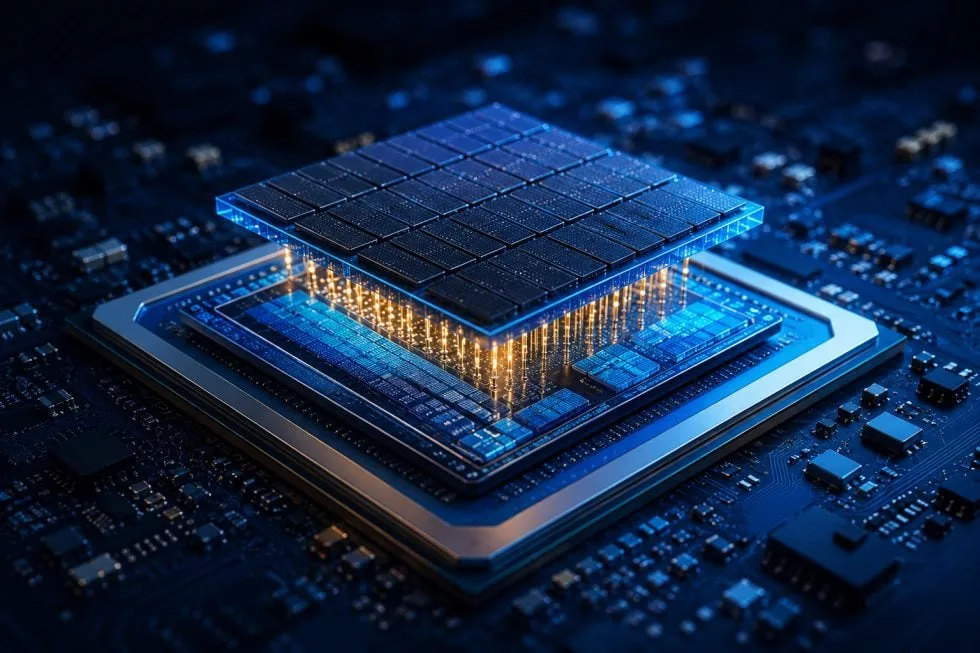
Intel is once again intensively exploring memory technologies. In a recent interview, CEO Lip-Bu Tan highlighted that new memory architectures offer significant potential for technical innovation. He specifically mentioned the possibility of tighter integration between memory and processors, including direct vertical stacking over compute chips. However, Intel has not announced a return to classic DRAM or NAND mass production.
Memory moves closer to compute units
The new considerations differ fundamentally from simply restarting a DRAM fab. Modern AI and HPC systems are increasingly bottlenecked by the speed of data movement between compute units and memory. Consequently, physical integration of logic, cache, and high-bandwidth memory is gaining importance.
The most prominent example is HBM (High Bandwidth Memory). Multiple DRAM dies are vertically stacked and connected to a processor or accelerator via wide interfaces. In current AI accelerators, these HBM stacks are located within the same complex package as the compute chip, though typically placed adjacent to it and connected via interposers or other packaging techniques.
Tan is now discussing even stronger integration: placing memory directly over a processor. This could further shorten trace lengths and increase available bandwidth. Technically, this would require 3D-stacking, very dense connections, and sophisticated heat dissipation. Tan did not specify the concrete technology, memory type, manufacturing process, products, or timeline.
Advanced Packaging strategy vs. DRAM production
The significance of Intel's comments is amplified by a recent personnel decision. In June 2026, the company brought back Seok-Hee Lee, former President and CEO of SK hynix. At Intel, Lee will serve as Executive Vice President of Intel Foundry, responsible for Advanced Packaging, system integration, backend technology development, and backend manufacturing.
Intel now positions Advanced Packaging as a standalone business unit. Tan's stated goal is to connect leading logic, memory, networking technologies, and other components more closely. Lee will focus on advancing technologies like EMIB (Embedded Multi-Die Interconnect Bridge) and HBM, which are crucial for efficiently connecting compute chips, I/O dies, and HBM in AI accelerators.
This is a strategy to deepen integration at the package level, not to build a new fab for standard DDR5 modules or NAND chips. The DRAM and NAND markets are dominated by few major players (Samsung, SK hynix, Micron for DRAM; Kioxia, SanDisk for NAND) with high capital expenditure requirements.
Official status: confirmed facts vs. speculation
It is crucial to distinguish between architectural research and production announcements. Intel has fully sold its NAND technology and manufacturing business to SK hynix, completing the second stage of the transaction on March 27, 2025 (receiving roughly $1.9 billion). The company also ceased development of future Optane products in 2022.
Tan's statements and Lee's appointment signal a strategic interest in new forms of memory integration using packaging competencies, not a return to standard memory chip production. This aligns with analysis from sources like Barron's and Tom's Hardware, which interpret the news as a potential signal for renewed strategic engagement with memory technologies via packaging, rather than an immediate decision to re-enter DRAM manufacturing.
Гика
