
RTX 5090 Mod: Two extra 8-Pin-Stecker to offload 12V-2x6
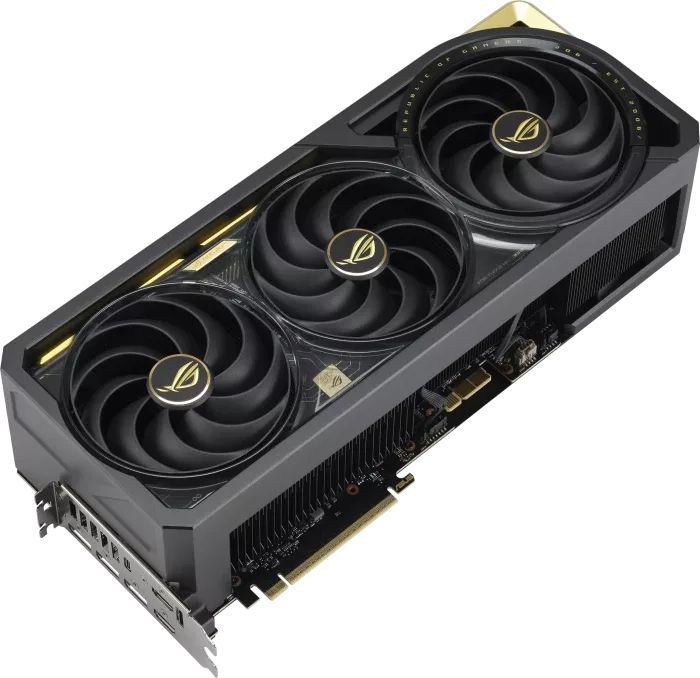
As power requirements for high-end GPUs climb, the density of power delivery through a single connector becomes a critical factor. A Reddit user known as DallasGrave has shared a custom modification for his MSI GeForce RTX 5090. Instead of replacing the existing 16-pin interface, the modder installed an adapter PCB that draws power from the original 12V-2x6 connector and distributes it to two additional PCIe-8-Pin sockets.
The principle behind this modification is straightforward: increasing the number of conductors and contact surfaces to reduce the current flowing through any single pin. At a 550W load, the current on the 12V side is theoretically quite high. If contact resistance is uneven, certain pins can experience significant heating. By providing more paths for the current, the user intends to mitigate this risk.
Experimental Results and Technical Context
According to the creator, the modified GeForce RTX 5090 ran for 48 hours under a 550W load without any monitored power lines exceeding 40 °C. While these results appear impressive, they must be viewed with caution. This is an unverified, single-user experiment, not a certified safety upgrade. The test was conducted at 550W, which is below the maximum 600W power limit some GeForce RTX 5090 cards can reach. Furthermore, there has been no independent electrical validation or testing with various power supplies to confirm the stability of this setup.
From an engineering perspective, the logic is sound. In parallel circuits, current distributes according to the resistance of the paths. More copper and more contacts generally lead to lower resistance and reduced heat dissipation, as power loss is calculated by the formula P = I² × R. However, the complexity of the modification introduces new variables, such as the quality of the solder joints and the integrity of the additional PCB.
Risks and Practical Advice
While the experiment demonstrates a plausible way to manage high current, it is far from a recommended consumer solution. Modifying the power delivery of an expensive graphics card carries significant risks: a single poor solder joint or an issue with grounding could cause more damage than the original connector issue. Additionally, such modifications will void any manufacturer warranty.
For the average user, the safest approach remains using high-quality, fully seated cables, avoiding sharp bends at the connector, and monitoring for any unusual temperatures or discoloration. This project serves as an interesting technical case study rather than a viable DIY solution for the general public.
Гика
