
TSMC plans High-NA EUV adoption by 2030 for A10 or A11 nodes
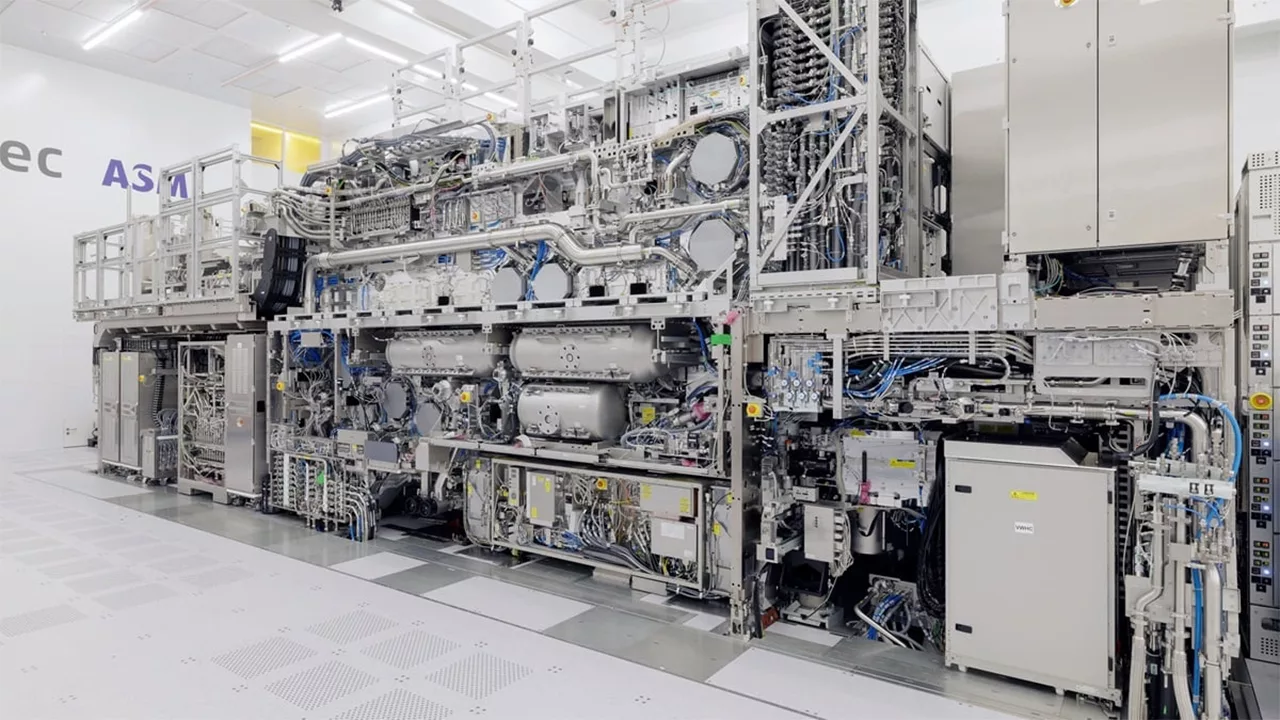
TSMC has officially confirmed it will begin using High-NA EUV lithography for high-volume manufacturing in 2030, marking a significant shift from its long-standing strategy of avoiding such expensive equipment. While the company previously relied on Low-NA EUV systems to maintain process advancement without investing in $400 million scanners, the complexity of modern transistor architectures—specifically gate-all-around (GAA) and future complementary field-effect transistors (CFETs)—now necessitates the higher resolution offered by High-NA optics. This transition is expected to coincide with the company's A10 or A11 technology nodes, which are prime candidates for adopting this new generation of ASML tools.
The Strategic Shift from Low-NA to High-NA
For years, TSMC successfully navigated the semiconductor manufacturing landscape by delaying the adoption of High-NA Extreme Ultraviolet (EUV) lithography. The primary driver for this caution was economic: High-NA scanners cost approximately $400 million each, a steep price tag that the company preferred to avoid if possible. Instead, TSMC relied on Low-NA EUV systems, which offered sufficient resolution for many years and allowed the foundry to advance its process technologies without immediately incurring massive capital expenditures. However, as transistor architectures become increasingly complex, particularly with the introduction of 3rd Generation nanosheet GAA transistors, the limitations of Low-NA systems have become apparent. The company has now acknowledged that it cannot rely on Low-NA EUV forever and has announced plans to integrate High-NA systems into its production line starting in 2030.
Timeline and Photomask Evolution
TSMC's roadmap for High-NA adoption is structured in distinct phases. The company plans to initiate high-volume manufacturing using High-NA EUV lithography with conventional 6×6-inch photomasks in 2030. This initial phase will allow TSMC to validate the technology and optimize yields before committing fully to the more advanced format. Following this, a pilot line utilizing larger 6×12-inch photomasks is scheduled for construction in 2031. The ultimate goal of this initiative is to bring 6×12-inch High-NA lithography systems into advanced node production by 2033. This gradual approach mirrors the industry's standard practice of ramping up new, expensive equipment carefully to ensure stability and cost-effectiveness.
Identifying the First Adopters: A10 or A11?
The most intriguing aspect of this announcement is determining which specific process technology will be the first to utilize High-NA EUV scanners for its most critical layers. TSMC has not formally revealed the exact node name, but analysis of their roadmap points strongly toward the A10 or A11 technologies as the prime candidates. These nodes fall into the 1/1.1nm-class category and are positioned to deliver substantial gains in transistor density, performance, and power efficiency. TSMC's current strategy divides its roadmap into annual client-oriented nodes (such as N2, N2P, N2X, A14, and A13) and roughly biennial high-performance nodes (like A16 in 2027 and A12 in 2029). Notably, the company has confirmed that the A12 and A13 nodes, arriving in 2029, will continue to rely on conventional Low-NA EUV lithography. Since A13 is an optical shrink of A14 with only a 6% increase in transistor density, its successor—likely designated as A11 or A10—will need to deliver considerably more significant improvements. This suggests that the transition to High-NA will be reserved for the node that requires the highest level of precision to achieve meaningful architectural breakthroughs.
ASML's Role and Industry Context
The implementation of High-NA EUV is a joint effort between TSMC and ASML, the Dutch manufacturer of lithography systems. ASML has expressed strong support for this initiative, noting the robust backing from semiconductor manufacturers, mask suppliers, and partners. The move to High-NA represents a critical step in the ongoing arms race for Moore's Law, as it allows for finer feature sizes that are essential for next-generation processors. While TSMC remains the leader in advanced packaging technologies like CoWoS and SoIC, the integration of High-NA EUV will be crucial for maintaining its edge in logic chip manufacturing against competitors like Intel and Samsung, who are also aggressively pursuing similar lithography advancements.
Гика
