

NVIDIA NVHBM: Up to 30% More Bandwidth for Custom AI Chips
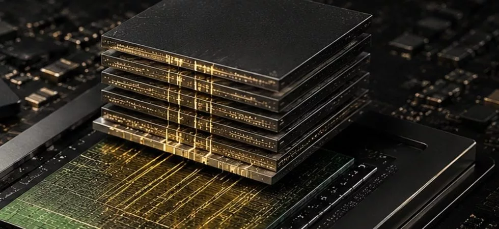
NVIDIA has unveiled a new memory technology called NVHBM, designed to solve a critical bottleneck in custom AI chip design: the massive silicon area consumed by High Bandwidth Memory (HBM) interfaces. Announced on August 26, 2026, as part of the broader NVLink Fusion initiative, this technology aims to integrate third-party AI accelerators—referred to by NVIDIA as XPUs—more deeply into its infrastructure ecosystem.
The core innovation of NVHBM lies in its architectural shift. Unlike standard HBM4E, which requires significant die area on the accelerator chip for PHYs, memory controllers, and wide I/O connections to the compute units, NVHBM relocates the memory controller deeper into the three-dimensional HBM stack itself. This structural change allows for narrower interconnects between the HBM and the main chip. NVIDIA claims this approach reduces the silicon footprint required for the PHY and associated support logic by up to 67%, while simultaneously freeing up to 25% more usable area on the Compute Die for additional matrix units, vector processors, or specialized functions.
These architectural changes translate into tangible performance metrics. Compared to standard HBM4E, NVHBM offers up to 30% higher memory bandwidth, which is crucial for large language models that must rapidly move weights and activations between compute units and memory. Additionally, the technology reduces HBM power consumption by up to 15%. While these individual improvements might seem incremental at a single-chip level, NVIDIA projects an end-to-end XPU performance boost of up to 30% when combining increased bandwidth, expanded compute area, and lower power draw.
Strategically, NVHBM is not primarily targeted at consumer GeForce or standard GPU lines. Instead, it serves the growing market of hyperscalers and enterprises developing custom AI chips, such as Google's TPUs, Amazon's Trainium and Inferentia, Microsoft's Maia, and OpenAI's Jalapeño. By providing a standardized interface that saves space and power, NVIDIA is attempting to ensure that even when customers build their own processors, the rest of the data center—networking, rack architecture, and software platforms—remains on NVIDIA's infrastructure.
Amazon's Annapurna Labs has been named as the first partner collaborating on this technology. The solution is part of a larger concept where custom CPUs and XPUs can be integrated into NVLink-based rack systems via an NVLink-Fusion chiplet. This allows NVIDIA to maintain control over the data center ecosystem, regardless of who manufactures the actual AI processor.
It is important to note that these figures are manufacturer specifications rather than independent benchmark results from finished systems. The 30% performance gain and other metrics represent theoretical potential based on architectural efficiency gains. Whether these improvements materialize in real-world deployments will depend on future product implementations and system-level optimizations.
In summary, NVHBM signals a significant shift in NVIDIA's strategy toward custom AI hardware. Rather than relying solely on customers purchasing off-the-shelf GPUs, the company is now offering specific building blocks to integrate external accelerators into its ecosystem. While technically promising, the real-world impact of shifting memory overhead into the stack and reclaiming compute area will be fully validated only when commercial products utilizing NVHBM are released.
Гика
