
Nvidia custom 'NVHBM' promises 30% higher bandwidth, 15% lower power than commodity HBM4e
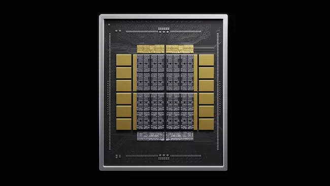
Nvidia has expanded its NVLink Fusion ecosystem by introducing a custom high-bandwidth memory solution called NVHBM. This new component is designed specifically for partners developing custom silicon, offering significant performance advantages over standard commodity HBM4e. The initiative aims to provide building blocks that allow partners to achieve higher bandwidth and lower power consumption in their AI accelerator designs.
Nvidia's NVLink Fusion program provides the necessary infrastructure for connecting custom chips into large-scale coherent systems, such as the Vera Rubin NVL72 rack-scale accelerator. Today, the company is adding a critical new component to this toolkit: NVHBM. As Nvidia describes it, this is not a replacement for standard HBM4e but rather a specialized implementation of high-bandwidth memory tailored for custom silicon developers.
The core promise of NVHBM lies in its efficiency metrics. Nvidia states that the custom solution delivers up to 30% higher bandwidth per stack compared to standard commodity HBM4e. Simultaneously, it claims a 15% reduction in power usage. These improvements are achieved through a custom base die and PHY design that moves the memory controller into the base die of the HBM stack itself. This architectural shift reduces the footprint of memory-related circuitry on the primary custom accelerator die, freeing up valuable silicon real estate.
For memory-bandwidth-bound AI workloads, these specifications translate directly into practical benefits. Higher bandwidth allows for increased throughput, such as a higher tokens-per-second rate for AI inference tasks. The power savings are equally significant; energy saved on data movement can be reinvested into higher performance from the accelerator itself or reallocated to support larger numbers of accelerators within the same fixed power envelope. This is particularly crucial for hyperscale installations moving massive data structures like model weights and KV caches across thousands of chips.
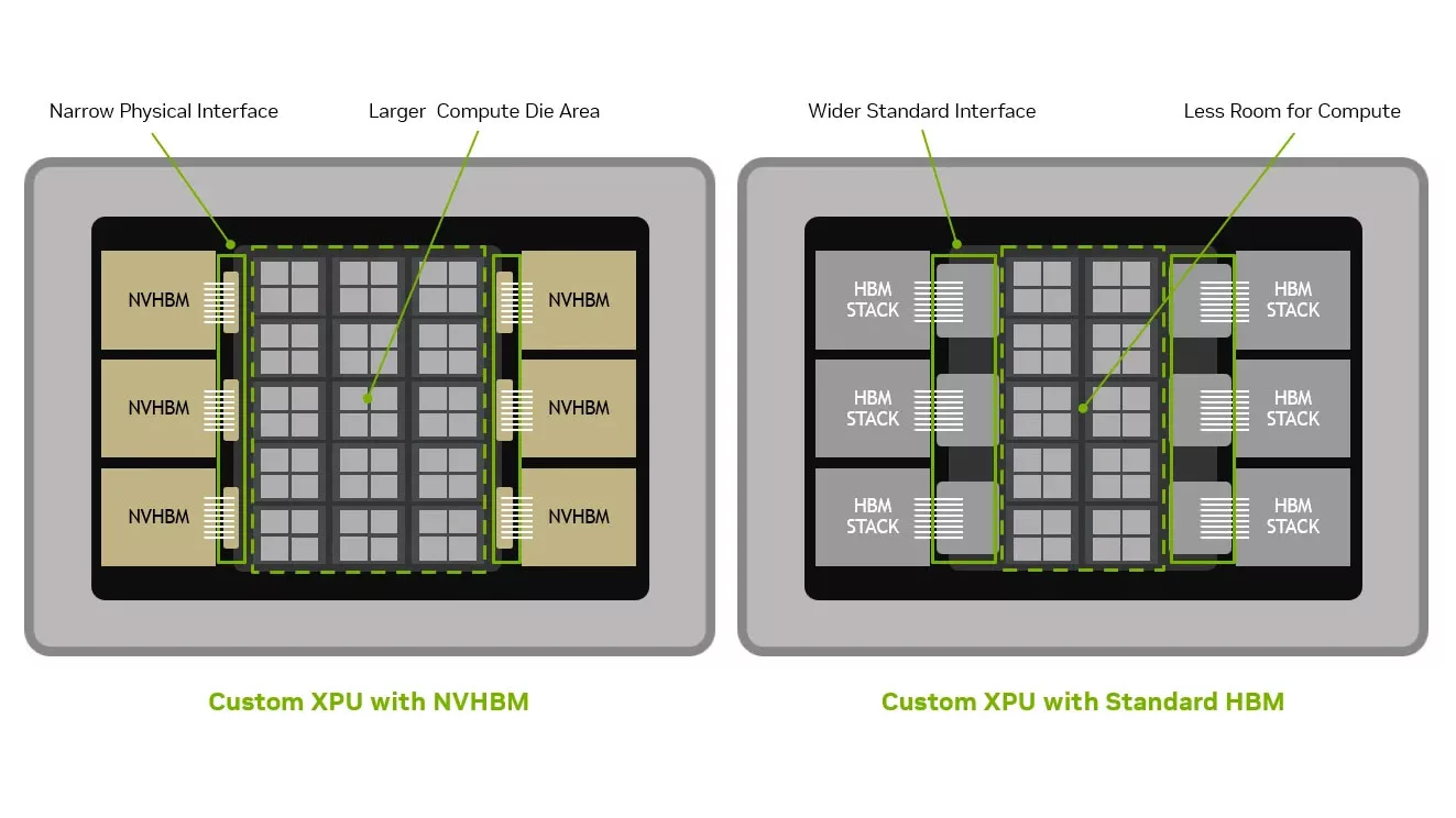
It is important to note that these benefits are targeted at Nvidia's prospective partners who are incorporating NVLink Fusion and NVHBM into their own custom designs, rather than existing Rubin rack-scale systems already in production. The technology is validated with "leading memory vendors," promising faster time-to-market for custom silicon developers compared to implementing commodity HBM from the ground up.
Amazon's Annapurna Labs has been announced as the first partner for NVHBM. Nafea Bshara, VP of Annapurna Labs, expressed enthusiasm for the collaboration, stating it will benefit future AWS infrastructure designs. Since Annapurna's next-generation Trainium 4 AI chips already support the NVLink Fusion scale-up interface, it is highly likely that follow-on chips will also support NVHBM.
While the technology offers a compelling path forward for custom silicon developers seeking to optimize performance-per-watt and throughput, it remains a specialized offering. The distinction between this custom implementation and standard commodity HBM4e ensures that the market retains flexibility while providing a high-performance option for those who can leverage Nvidia's specific architectural advantages.
Гика
