AMD Zen 6 Architecture Deep Dive: A New Era of Core Design
AMD has officially unveiled the EPYC 9006 series, marking the debut of the Zen 6 architecture in the server and data center market. While consumer Ryzen processors await their turn, the technical details revealed during recent architecture briefings offer a fascinating glimpse into how AMD is evolving its silicon to meet the demands of modern computing. This deep dive explores the fundamental shifts in the Zen 6 and Zen 6c designs, from the front-end improvements to the radical restructuring of the integer scheduler.
The arrival of the Zen 6 architecture marks a significant departure from previous generations. Historically, AMD has introduced new Zen architectures through the Ryzen consumer brand first, followed by EPYC server processors. However, with Zen 6, the priority has shifted toward the data center. The EPYC 9006 series, codenamed 'Venice,' began shipping in November 2026 for the Socket SP7 platform, driven by the intense industry demand for AI-optimized data center solutions.
While desktop gamers are still waiting for official mentions of Zen 6-based Ryzen CPUs, the architectural blueprints provided during the recent briefing in Las Vegas offer a clear picture of what is coming. The architecture is split into two distinct profiles: the standard Zen 6 and the compact Zen 6c. Unlike the Zen 5c, which was essentially a cache-reduced version of the standard core, Zen 6 and Zen 6c are being designed with different fundamental goals in mind.
Two Paths: Zen 6 vs. Zen 6c
According to Mike Clark, Lead "Zen" Architect at AMD, the Zen 6 core is optimized for high clock speeds, aiming to deliver low-latency, high single-threaded performance. In contrast, the Zen 6c core prioritizes Instructions Per Cycle (IPC) and power efficiency over raw frequency. Both cores are manufactured using TSMC's 2nm-class 'N2P' process.
- Zen 6 CCD: 12 cores / 24 threads (Max clock: 5.3GHz)
- Zen 6c CCD: 32 cores / 64 threads (Max clock: 4.1GHz)
- Manufacturing Process: TSMC N2P (2nm-class)
The architectural divergence is significant. While the Zen 6c CCD is much larger to accommodate the high core count, the standard Zen 6 CCD is designed for the high-frequency demands of desktop gaming. It is highly probable that top-tier Ryzen 9 processors will utilize two Zen 6 CCDs to achieve a 24-core, 48-thread configuration.
Front-End Enhancements and Op Fusion
The front-end of the Zen 6 architecture shows targeted improvements rather than a total overhaul. The instruction fetch width remains at 32 bytes x 2, matching the Zen 5 design. However, the branch predictor has received upgrades, specifically the expansion of the Return Address Stack (RAS) from 52 to 64 entries to better support the larger out-of-order execution windows.
One of the most critical changes is in the Micro-Op (μOP) Cache. While the total number of entries in the Op Cache has actually decreased from 1,024 in Zen 5 to 768 in Zen 6, the throughput has increased significantly. The Op Cache output width has jumped from 12 μOPs per cycle to 18 μOPs per cycle. This is made possible by a feature called 'Increased Op Fusion,' which allows the decoder to combine multiple x86 instructions into a single, more efficient μOP.
This redesign means that even with fewer cache entries, Zen 6 can process more complex x86 instruction sequences in parallel, effectively increasing the work done per clock cycle compared to its predecessor.
A Radical Redesign of the Integer Scheduler
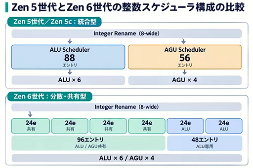
The most profound change in the Zen 6 architecture lies in the integer execution engine and its scheduler. In previous generations like Zen 5, the scheduler was split into two rigid pools: one for Arithmetic Logic Units (ALU) and one for Address Generation Units (AGU). This meant that if one pool was full while the other was empty, the CPU could not dynamically reallocate those resources, leading to inefficiencies.
Zen 6 solves this by implementing a more flexible, unified scheduling approach. Instead of fixed pools, the architecture uses a series of 24-entry schedulers. A portion of these are dedicated to both ALU and AGU operations (96 entries total), while the remaining 48 entries are reserved specifically for ALU tasks. This allows the CPU to dynamically balance the workload between address calculation and mathematical operations based on the specific needs of the software.
This shift from rigid, specialized pools to a flexible, multi-purpose scheduling system is a direct response to the evolving nature of modern workloads, which increasingly demand a mix of heavy integer math and complex memory addressing for AI, gaming, and server-side applications.
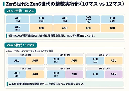
The architectural refinements in Zen 6 extend deep into the execution engine. While the number of ALUs (6) and AGUs (4) remains consistent with the Zen 5 generation, the way instructions are handled has evolved. In Zen 5, branch units were shared with ALUs, potentially causing contention between integer arithmetic and branch instructions. Zen 6 addresses this by introducing two independent Branch Units (BRN), allowing branch instructions and integer operations to be processed in parallel more effectively.
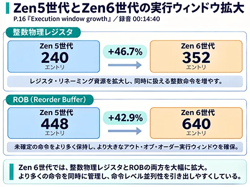
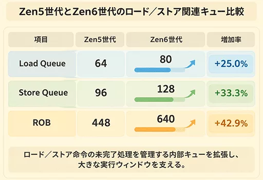
To optimize die area and reflect modern software trends, AMD has made some strategic reductions. The number of multipliers has been cut from three in Zen 5 to two in Zen 6. This reduction coincides with the restructuring of execution units into six blocks to accommodate the 144-entry scheduler. Additionally, to boost out-of-order execution efficiency, the Physical Register File (PRF) and the Reorder Buffer (ROB) have both been expanded by more than 1.4x compared to Zen 5, increasing the window for instruction reordering and improving IPC.
Floating-Point Evolution: Zen 6 vs. Zen 6c
The Floating-Point (FP) block sees significant structural changes, particularly in the scheduler. Zen 6 increases its FP scheduler capacity to 46 entries per unit (3 units total), while the Zen 6c variant jumps to 60 entries per unit. This makes the total FP scheduler capacity 138 entries for Zen 6, compared to 180 entries for Zen 6c. This expansion is designed to increase the utilization of FP execution units by allowing the CPU to hold more independent instructions, reducing idle time during complex dependency chains.
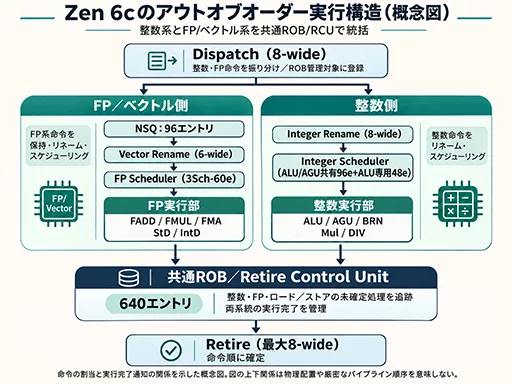
The distinction between Zen 6 and Zen 6c is driven by a fundamental trade-off between clock speed and IPC. According to AMD, Zen 6 is optimized for high clock speeds, targeting up to 5.3GHz. To achieve this, the blocks are kept smaller to minimize signal propagation delay. In contrast, Zen 6c targets a lower maximum frequency of 4.1GHz, allowing for larger, more complex schedulers that prioritize Instruction Per Clock (IPC) over raw frequency.
Memory Subsystem and Load/Store Enhancements
Zen 6 introduces critical improvements to the Load/Store (LS) pipeline to meet the demands of SIMD-heavy modern software. A major highlight is the ability to execute four 256-bit loads per clock cycle. While Zen 5 had the necessary 1024-bit bus width, it could only handle two 256-bit loads per cycle due to control logic complexities. By optimizing this, Zen 6 can achieve up to twice the peak load performance for legacy AVX2 workloads compared to Zen 5. However, store performance remains unchanged, limited to one 512-bit or two 256-bit writes per cycle, with improvements deferred to Zen 7.
To further enhance Memory-Level Parallelism (MLP), the Load/Store Queues have been expanded. The Load Queue grows from 64 entries in Zen 5 to 80 entries in Zen 6, while the Store Queue increases from 96 to 128 entries. These expansions, working in tandem with the larger ROB, allow the CPU to manage more outstanding memory requests, which is vital for maintaining performance during L1 cache misses.
Cache Hierarchy and CCD Scaling
The cache structure shows a significant scaling effort, particularly in the Zen 6c variant. While the L1 and L2 cache specifications remain identical to Zen 5 (48KB L1D and 1MB L2), the L3 cache and core density have seen massive shifts. In the Zen 6c design, the number of cores per CCD has doubled to 32, and the L3 cache capacity has quadrupled to 128MB. Notably, Zen 6c restores the 4MB-per-core L3 ratio seen in Zen 6, moving away from the reduced ratio used in Zen 5c to ensure efficient data sharing across its high core count.
AMD has also refined L2 cache access efficiency. To prevent excessive prefetching from consuming L2 bandwidth and conflicting with standard read operations, the arbitration and prefetch control mechanisms have been redesigned. This is particularly crucial for the high-density Zen 6c CCDs, where massive amounts of prefetch requests from many cores could otherwise saturate the L2 bandwidth.
The evolution of AMD's processor lineup is increasingly defined by a strategic divergence in core design. Recent technical deep dives into the upcoming Zen 6 architecture reveal that AMD is moving toward a more specialized approach, distinguishing between the standard Zen 6 and the efficiency-oriented Zen 6c. This distinction is not merely a matter of clock speeds or power limits, but a fundamental difference at the architectural level.
Architectural Bifurcation: Zen 6 vs. Zen 6c
The core of AMD's strategy lies in how these two variants will serve different market segments. While the standard Zen 6 is designed to push the boundaries of single-core performance and high-frequency throughput for demanding desktop and enthusiast workloads, the Zen 6c is being engineered with a focus on area efficiency and power-to-performance optimization. This makes the 'c' variant particularly suited for high-density computing environments, such as laptops or high-core-count server configurations, where physical space and thermal management are critical constraints.
This architectural split allows AMD to optimize the silicon layout for specific use cases. By tailoring the physical implementation of the cores—potentially adjusting the size of caches or the complexity of the instruction pipeline—AMD aims to provide a more versatile product stack. This ensures that whether a user requires raw computational power or sustained efficiency in a compact form factor, the underlying Zen 6 instruction set architecture (ISA) remains consistent while the physical execution varies.