

AMD Verano: 192 N2P-Kerne, 500W TDP, and Two Dummy Chips in SB1 Socket
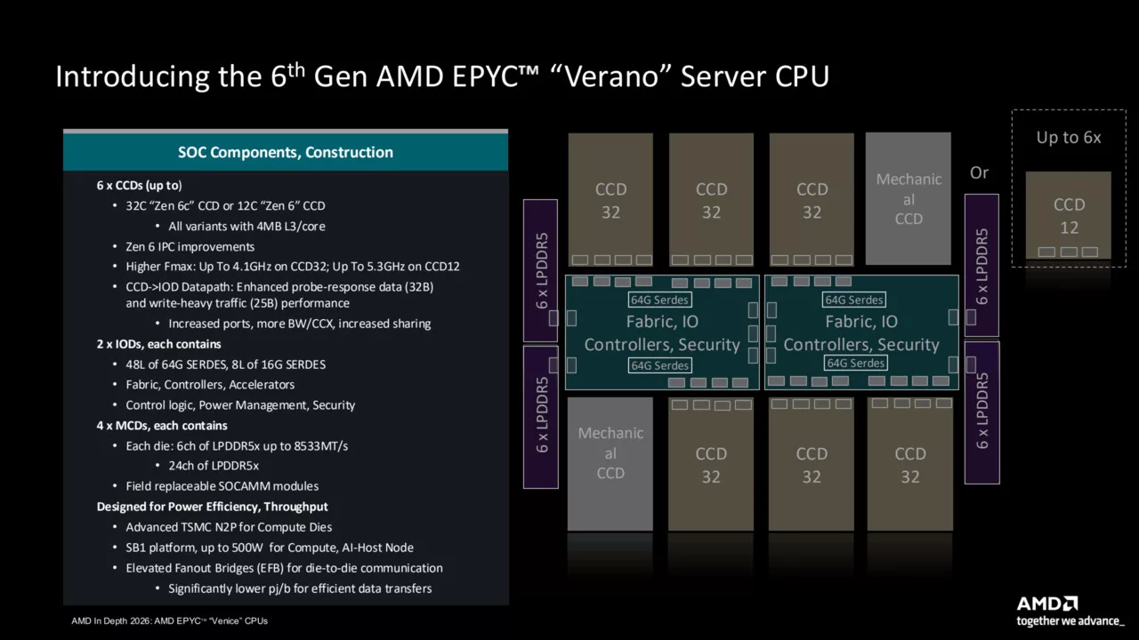
AMD is moving deeper into the high-performance computing landscape with new details regarding the Verano processor. Based on the Zen 6 architecture, this Epyc CPU is designed to challenge competitors by utilizing TSMC's N2P process and a specialized IO Die architecture that introduces LPDDR5X support to the lineup.
The Verano chip, which has been teased at recent tech events, represents a significant shift in AMD's server strategy. Unlike the Venice architecture, Verano utilizes a unique configuration of six CCDs instead of eight. To maintain the physical package layout, AMD is employing two dummy dies to fill the gaps, ensuring the chip maintains its structural integrity while focusing resources on the active silicon.
A New IO Die and LPDDR5X Support
One of the most critical technical changes is the introduction of a third type of IO Die for the Epyc 9006 series, specifically designed for the SB1 socket. This new design addresses the limitations of previous IO Dies used in the SP7 and SP8 sockets. The Verano package will feature two IO Dies containing a total of four MCDs (Memory Controller Dies). Each MCD manages six channels of LPDDR5X, resulting in a massive 24-channel memory configuration.
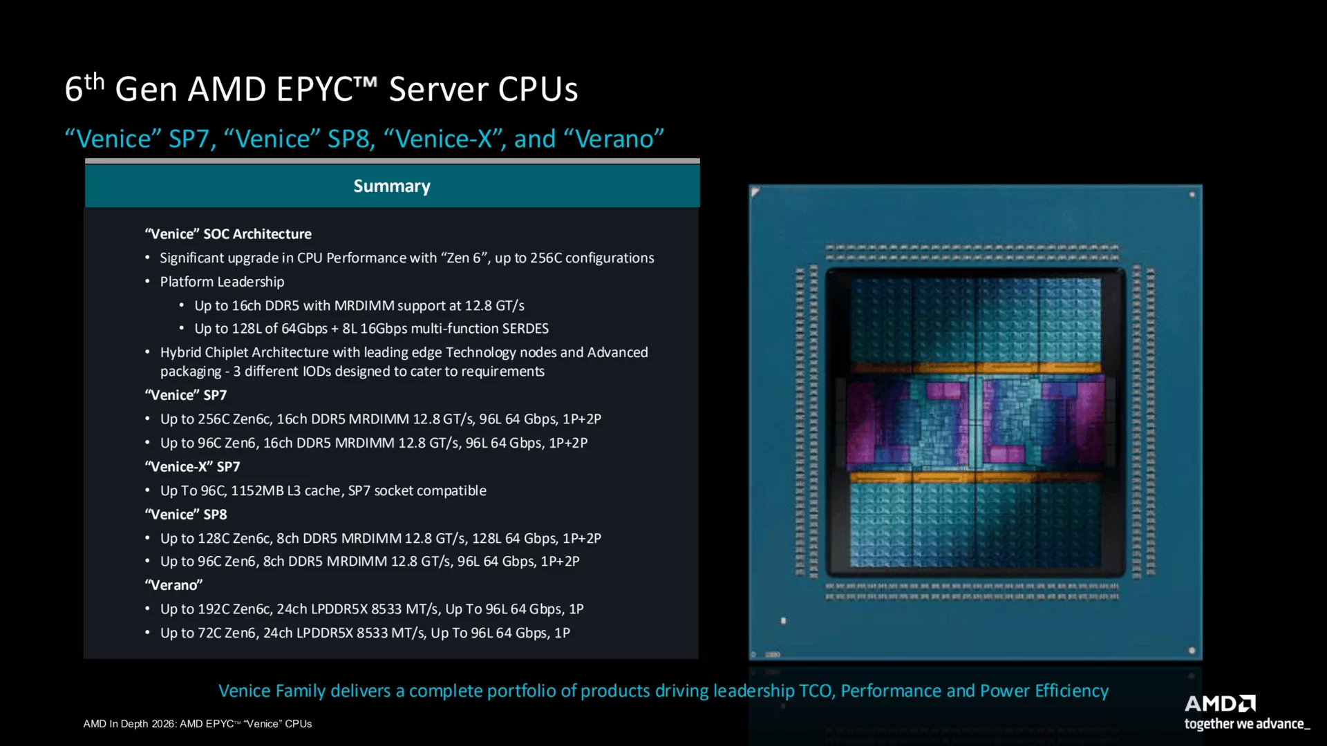
AMD has officially specified LPDDR5X-8533 support via the replaceable SOCAMM2 interface. However, historical trends suggest that memory clock speeds might see further increases shortly before the product's launch. This high-bandwidth memory support positions Verano as a high-performance host CPU, potentially serving as the backbone for massive GPU clusters, similar to how the current Epyc processors support Instinct accelerators in the AMD Helios racks.
Core Configuration and Thermal Profile
The core count for Verano depends on the specific CCD implementation used. The processor can feature up to 192 Zen 6c cores (using six CCD32 dies) or 72 Zen 6 cores (using six CCD12 dies). Notably, the dummy dies do not provide additional features; they are strictly for package consistency and do not offer the same feature set as the active CCDs. Regarding power, Verano is rated at a 500W TDP. While this is lower than the 600W maximum seen in Venice, the reduction in core count per package allows for higher clock speeds on the active silicon.
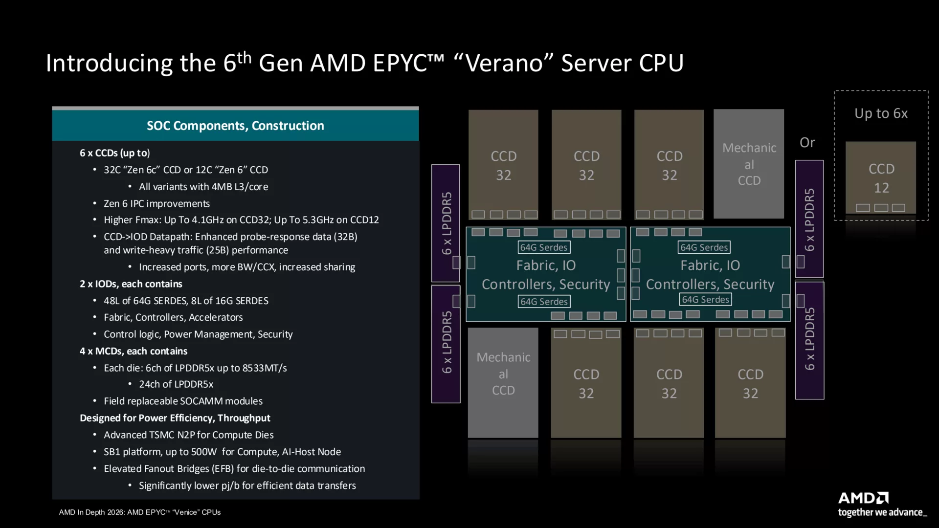
AMD expects to begin offering these processors in the second half of 2027, though a release as early as the first half of that year remains a possibility according to OCP statements. For now, the SB1 socket is designed for single-socket operation, meaning Verano will not support dual-socket configurations.
Гика
