

TinyGPU v2.0 on Real Silicon: 1.000 Triangles
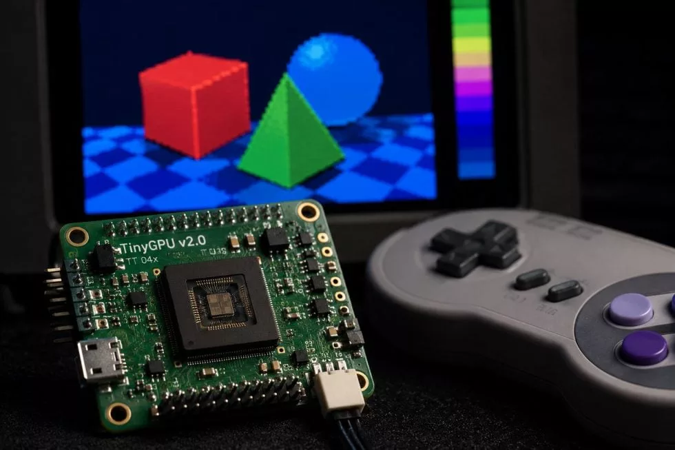
Developers of the TinyGPU project have successfully transitioned from experimental FPGA prototypes to a manufactured silicon chip. The chip, named TinyGPU v2.0, was demonstrated under the Tiny Tapeout initiative. Developer Pongsagon Vichit confirmed that the new version works correctly on real silicon, delivering results consistent with previous tests.
Performance and Specifications
The new TinyGPU v2.0 chip is not intended to be a modern gaming graphics card. It is an open-source project demonstrating key stages of classic 3D graphics in a compact Verilog implementation. The basic feature set includes transformation and lighting of 3D geometry, rasterization, backface culling, depth buffering, and flat shading with a dynamic directional light source.
Performance was measured at a resolution of 320 × 240 pixels. Under maximum load, a scene consisting of 1.000 triangles is rendered at approximately 6.5 frames per second (FPS). The color depth is limited to 4 bits, allowing the display of up to 16 colors simultaneously. The chip's operating frequency is 25.175 MHz (rounded to 25 MHz).
A 4-bit double buffer is used for image output, while an 8-bit Z-buffer stores depth values. Both types of memory are located in external QSPI-RAM connected to the chip, which helps save silicon area. Models are also loaded from external Flash memory. Control is handled via a connected SNES controller.
It is important to note that the performance of the real silicon chip does not exceed the FPGA prototype's benchmarks. This is an expected result: the project's success lies in the fact that all designed logic and memory architecture work without critical errors after manufacturing. Unlike FPGA, where errors can be fixed by loading a new configuration, on ASIC (application-specific integrated circuit) corrections require re-manufacturing the chip.
Technical Details and Code
The project's source code is open and available on GitHub under the Apache 2.0 license. The primary language for describing logic is Verilog. The repository contains modules for VGA output, SPI-Flash handling, color palette management, mathematical operations, and gamepad connection. This transparency allows researchers to study data paths and state machines directly.
The TinyGPU v2.0 chip occupies an area of 4 × 4 tiles on the Tiny Tapeout fab. This platform combines many small projects on a single wafer, distributing high manufacturing costs among participants. The project uses approximately 200,000 transistors (according to the developer) or up to 240,000 (according to Tom's Hardware). The difference in figures may be due to different methods of counting logic and standard cells.
Architectural Features
TinyGPU v2.0 does not use programmable shaders like modern graphics processors. Instead, graphics functions are implemented through specialized hardware paths. The architecture resembles early 3D accelerators with a fixed functional pipeline, rather than modern GPUs with shader arrays and free-floating compute units.
This limitation makes the architecture understandable: one can trace the path from vertex data through transformation, lighting, triangle construction, visibility testing, and rasterization to the final VGA signal. The project is positioned not as a product for embedded devices, but as a working model of a minimal 3D architecture.
Гика
