
Intel 14A Process Advances Toward Production With PDK 0.9
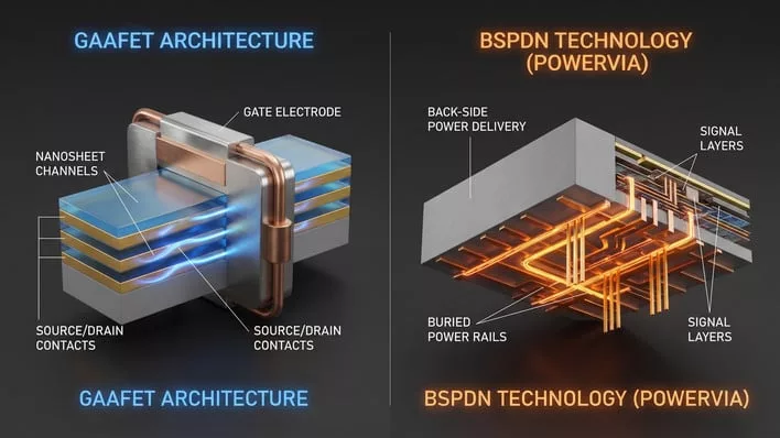
Intel Foundry is maintaining its aggressive roadmap toward sub-nanometer manufacturing. The company has officially released version 0.9 of its Intel 14A Process Design Kit (PDK), bringing its cutting-edge node one step closer to full-scale commercial production.
While the term PDK (Process Design Kit) might be obscure to non-engineers, it serves as the essential rulebook for chip manufacturing. It translates a fabrication plant's capabilities into digital building blocks that Electronic Design Automation (EDA) tools can interpret. Reaching version 0.9 signifies that the 14A node has matured significantly. Most importantly, this release includes 'Silicon-Backed Validation,' meaning the design rules have been verified against real silicon test chips rather than just theoretical simulations. This provides customers with the necessary confidence to begin developing complex, commercial-grade designs.
Architectural Leap: RibbonFET and PowerDirect
The 14A node represents a massive shift in transistor architecture, integrating the second generation of RibbonFET (GAAFET) and back-side power delivery (BSPDN) technology, now known as PowerDirect. According to Intel, the combination of RibbonFET 2 and PowerDirect offers substantial improvements over the 18A process:
With PDK 0.9 now in the hands of key partners, Intel is staying on track with its broader commercial timeline. This release reinforces the company's momentum as it moves toward full production readiness for its next-generation silicon.
Гика
